
PCBs are now used in almost all manufactured goods such as cars, cell phones, personal computers, among others. Let us know the manufacturing process of Printed Circuit Boards.
Summary of the Manufacturing Process of PCB:
PCBs are initially manufactured with the use of two types of software. Aided Design software (CAD) is used to design electronic circuit diagram to be produced. After the layout is designed, software manufacturing (CAM) computer aided is used by engineers to produce the prototype PCB.
Once the prototype PCB is designed, the first step in the manufacturing process is to select the material of the printed circuit board. There are many different types of PCB materials available, but the most popular, based on the application and requirements of a client, include: alumina, Arlon, Bakelite, CEM1, CEM5, ceramics, FR1, FR4, FR4 high temperature, Getek, Nelco, polyimide and the design requirement dictates Rogers. The size of the PCB (i.e.: length, width and thickness).
After the material has been selected, the first process is to apply a copper coating to the entire board. The circuit will then be printed on the card by a photoresist process. Then a photo etching process is used for all the copper that is not part of the circuit layout will be recorded or removed from the board. The resulting copper traces or tracks create the PCB circuit. To connect circuit traces, two processes are used. A mechanical milling process used CNC machines to eliminate unnecessary copper board. Then a, silkscreen, corrosion resistant, the printing process is applied to cover the regions in which traces must exist.
The PCB contains copper traces without any circuit components. To assemble the components, the holes will be drilled at points in electrical and electronic components are placed on the board. The holes are drilled with laser or a special type of drill bit made of tungsten carbide. Once the holes are drilled, hollow rivets are inserted into them or they are covered by an electroplating process, which creates the electrical connection between the layers of the board. A masking material is then applied to the entire layer except PCB pads and holes. There are many types of material masking such as lead solder, lead-free solder, OSP (Entek), deep/hard gold (electro-less gold nickel), immersion gold (electro-less gold nickel – ENIG), gold bondable (almost 99.99% pure gold), immersion silver, gold flash, immersion tin (tin white), carbon ink, and SN 100CL, an alloy of tin, copper, and nickel. The final step in the manufacturing process of PCB board is to screen print for labels and legend appear in the appropriate place.
Test the Quality of the PCB:
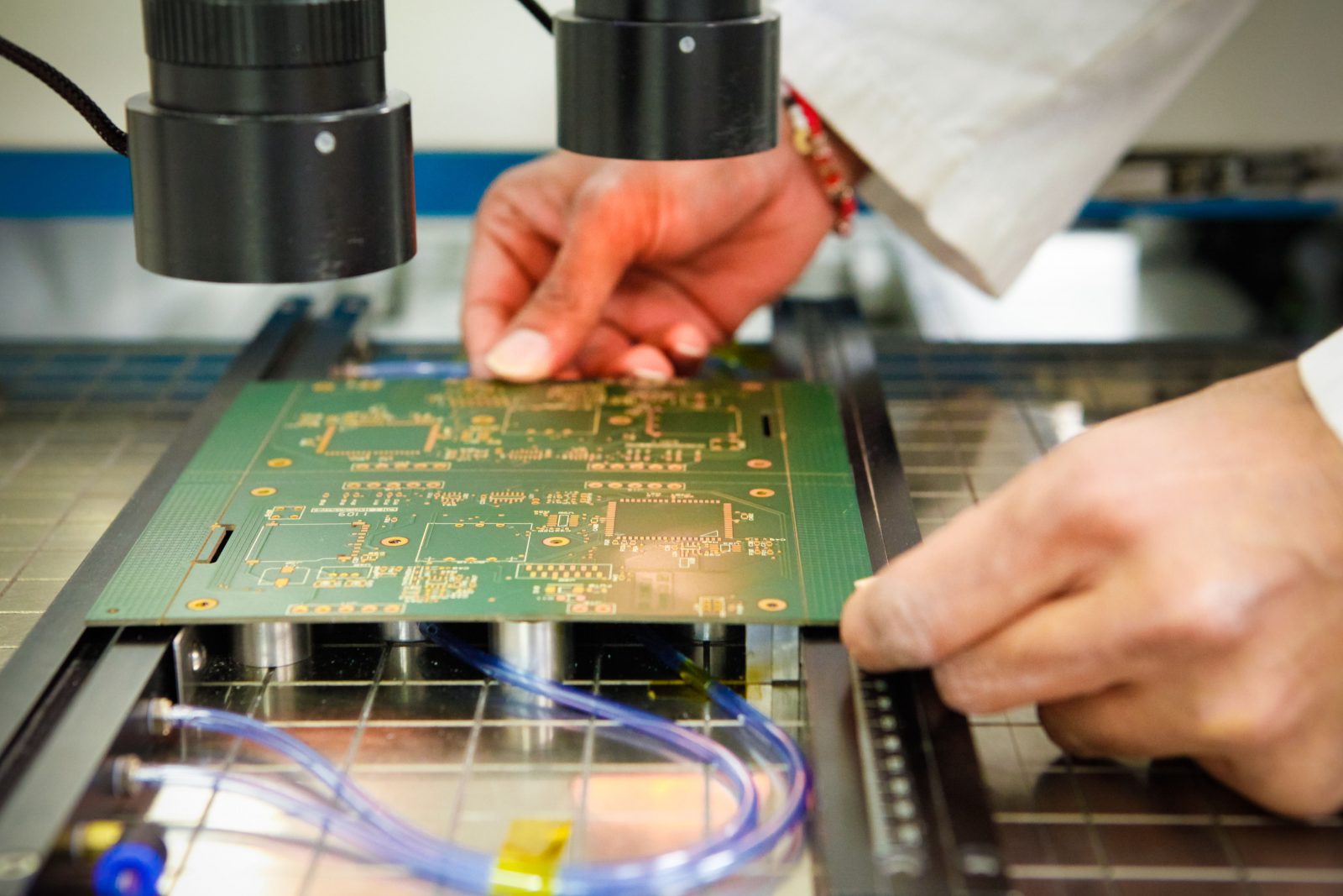
Before placing electrical and electronic components on the PCB, the board must be tested to verify functionality. In general, there are two types of failures that can cause a faulty PCB: short or open. A “short” is a connection between two or more points in the circuit that should not exist. An “open” is a point that there must be a connection, but does not. These defects should be corrected before mounting the PCB. Unfortunately, some manufacturers do not test their boards PCB before being shipped, which can lead to problems in the customer’s location.
This information has been shared on behalf of GradConn (www.gradconn.com), is offering a wide variety of custom cable assemblies, coaxial cable assemblies, with particular strength in micro coaxial cables for wireless markets, such as GSM, GPS, Wireless LAN (WLAN), Wi-Fi and Bluetooth.